- 您现在的位置:买卖IC网 > Sheet目录327 > HW-V5-ML561-UNI-G (Xilinx Inc)EVALUATION PLATFORM VIRTEX-5
Appendix C: LCD Interface
R
Table C-1:
Display Controller Specifications
Parameter
Supply Voltage
LCD Driving Voltage
Power Consumption
Sleep Mode
Standby Mode
Specification
2.4V to 3.6V (V DD )
4V to 15V (V LCD = V0 - V DD )
70 μ A typical (V DD = 3V, x4 boost, V0 = 11V,
internal supply = ON)
2 μ A
10 μ A
The on-chip RAM size is 65 x 132 = 8580 bits.
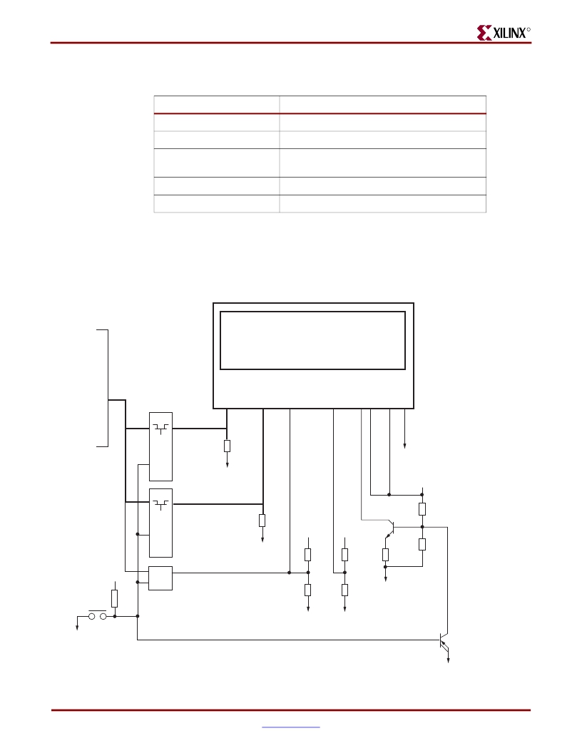
Hardware Schematic Diagram
LCD-BU S
LED
R s t
MI
- + Vcc Gnd
LCD_D[7:0]
IC19
3.3V
ENA, R/W, R S EL, C S 1B
IC22
3.3V
3.3V
68xx
3.3V
IC23
68xx
DIP1_4
Def au lt =
Def au lt = 68xx
Re s i s tor to Gnd
B a cklight ON/OFF
UG199_C_01_050106
Figure C-1:
Display Schematic Diagram
120
Virtex-5 FPGA ML561 User Guide
UG199 (v1.2.1) June 15, 2009
发布紧急采购,3分钟左右您将得到回复。
相关PDF资料
I-JET
JTAG ARM DEBUGGING PROBE
IAC24A
INPUT MODULE AC 5MA 24VDC
IAC5EQ
INPUT MODULE AC 10MA 5VDC
IB8RM
SURGE SUPP 8OUT 12'CORD W/REMOTE
IBAR12-20T
SURGE SUPPRSSR 20A 12OUT RACKMNT
IBAR12/20ULTRA
SURGE SUPPRSSR 20A 12OUT RACKMNT
IBAR12ULTRA
SURGE SUPPRSSR 15A 12OUT RACKMNT
IBAR12
SURGE SUPPRSSR 15A 12OUT RACKMNT
相关代理商/技术参数
HW-V5-ML561-UNI-G-J
功能描述:EVALUATION PLATFORM VIRTEX-5 RoHS:是 类别:编程器,开发系统 >> 通用嵌入式开发板和套件(MCU、DSP、FPGA、CPLD等) 系列:Virtex®-5 LXT 产品培训模块:Blackfin® Processor Core Architecture Overview
Blackfin® Device Drivers
Blackfin® Optimizations for Performance and Power Consumption
Blackfin® System Services 特色产品:Blackfin? BF50x Series Processors 标准包装:1 系列:Blackfin® 类型:DSP 适用于相关产品:ADSP-BF548 所含物品:板,软件,4x4 键盘,光学拨轮,QVGA 触摸屏 LCD 和 40G 硬盘 配用:ADZS-BFBLUET-EZEXT-ND - EZ-EXTENDER DAUGHTERBOARDADZS-BFLLCD-EZEXT-ND - BOARD EXT LANDSCAP LCD INTERFACE 相关产品:ADSP-BF542BBCZ-4A-ND - IC DSP 16BIT 400MHZ 400CSBGAADSP-BF544MBBCZ-5M-ND - IC DSP 16BIT 533MHZ MDDR 400CBGAADSP-BF542MBBCZ-5M-ND - IC DSP 16BIT 533MHZ MDDR 400CBGAADSP-BF542KBCZ-6A-ND - IC DSP 16BIT 600MHZ 400CSBGAADSP-BF547MBBCZ-5M-ND - IC DSP 16BIT 533MHZ MDDR 400CBGAADSP-BF548BBCZ-5A-ND - IC DSP 16BIT 533MHZ 400CSBGAADSP-BF547BBCZ-5A-ND - IC DSP 16BIT 533MHZ 400CSBGAADSP-BF544BBCZ-5A-ND - IC DSP 16BIT 533MHZ 400CSBGAADSP-BF542BBCZ-5A-ND - IC DSP 16BIT 533MHZ 400CSBGA
HW-V5-PCIE2-UNI-G
功能描述:KIT DEV PCIEXPRESS GTX VIRTEX5 RoHS:是 类别:编程器,开发系统 >> 通用嵌入式开发板和套件(MCU、DSP、FPGA、CPLD等) 系列:Virtex® -5 产品培训模块:Blackfin® Processor Core Architecture Overview
Blackfin® Device Drivers
Blackfin® Optimizations for Performance and Power Consumption
Blackfin® System Services 特色产品:Blackfin? BF50x Series Processors 标准包装:1 系列:Blackfin® 类型:DSP 适用于相关产品:ADSP-BF548 所含物品:板,软件,4x4 键盘,光学拨轮,QVGA 触摸屏 LCD 和 40G 硬盘 配用:ADZS-BFBLUET-EZEXT-ND - EZ-EXTENDER DAUGHTERBOARDADZS-BFLLCD-EZEXT-ND - BOARD EXT LANDSCAP LCD INTERFACE 相关产品:ADSP-BF542BBCZ-4A-ND - IC DSP 16BIT 400MHZ 400CSBGAADSP-BF544MBBCZ-5M-ND - IC DSP 16BIT 533MHZ MDDR 400CBGAADSP-BF542MBBCZ-5M-ND - IC DSP 16BIT 533MHZ MDDR 400CBGAADSP-BF542KBCZ-6A-ND - IC DSP 16BIT 600MHZ 400CSBGAADSP-BF547MBBCZ-5M-ND - IC DSP 16BIT 533MHZ MDDR 400CBGAADSP-BF548BBCZ-5A-ND - IC DSP 16BIT 533MHZ 400CSBGAADSP-BF547BBCZ-5A-ND - IC DSP 16BIT 533MHZ 400CSBGAADSP-BF544BBCZ-5A-ND - IC DSP 16BIT 533MHZ 400CSBGAADSP-BF542BBCZ-5A-ND - IC DSP 16BIT 533MHZ 400CSBGA
HW-VID-KIT
功能描述:可编程逻辑 IC 开发工具 Lattice Video Interface Kit
RoHS:否 制造商:Altera Corporation 产品:Development Kits 类型:FPGA 工具用于评估:5CEFA7F3 接口类型: 工作电源电压:
HW-VL1
制造商:IDEC CORPORATION 功能描述:BARRIER
HW-VL2
制造商:IDEC Corporation 功能描述:COVER;HW FNGR SAFE CONTAC CVR 制造商:IDEC CORPORATION 功能描述:HW FNGR SAFE CONTAC CVR
HW-VL3
制造商:IDEC Corporation 功能描述: 制造商:IDEC Corporation 功能描述:Replacs TW-VL3 FNGR SAF
HWW-X030T-10015Z-H1
制造商:P-TEC 制造商全称:P-tec Corporation 功能描述:X30T RGB LED Wall Washers
HWW-X030T-10015Z-H2
制造商:P-TEC 制造商全称:P-tec Corporation 功能描述:X30T RGB LED Wall Washers
